Main board
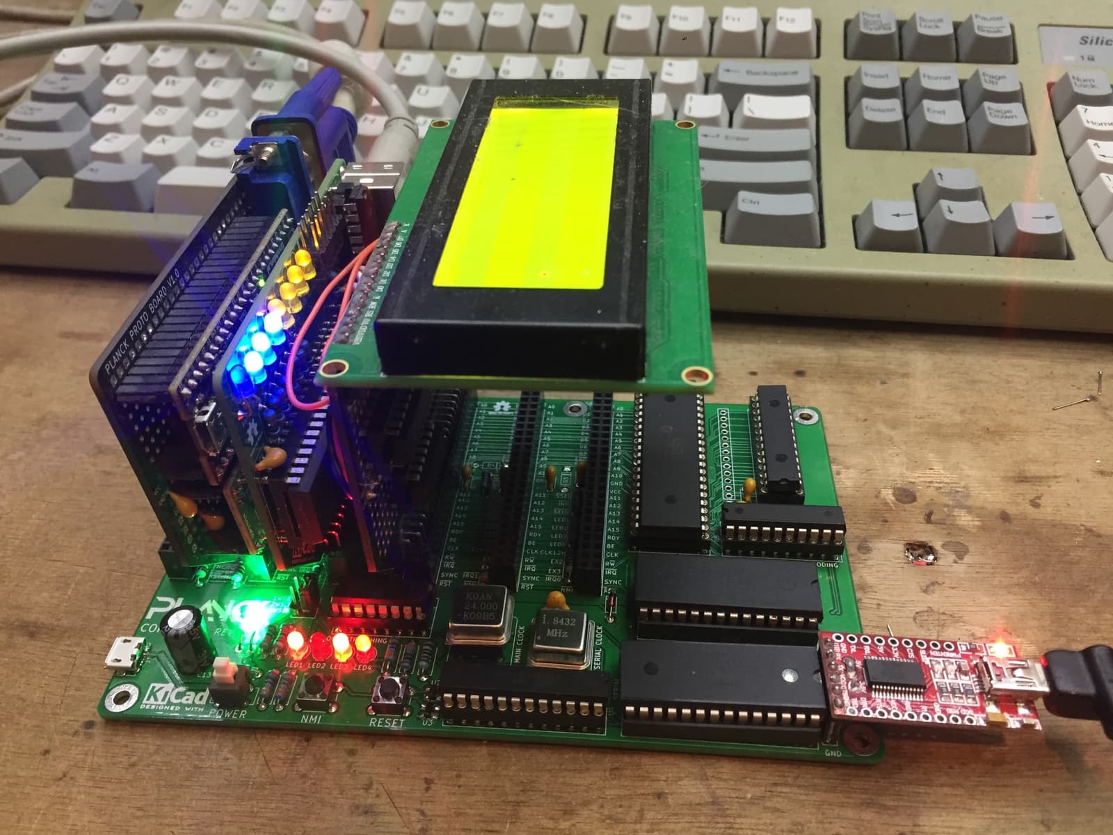
The Planck computer is an extensible single board computer. Everything need for the computer to work is on the mainboard (Basic IO, ROM, RAM, CPU). It can be extended with up to 6 cards to make it into exactly the computer you want.
The main board
Here are some details about the various subsystems on the main board.
Clock generation
The clock generation starts with an oscillator. This oscillator should be at twice the target frequency since it is divided by two by a 74HC161 binary counter
This counter makes possible the clock stretching that will be required by slow peripherals, or indeed any ROM if you run your computer fast enough.
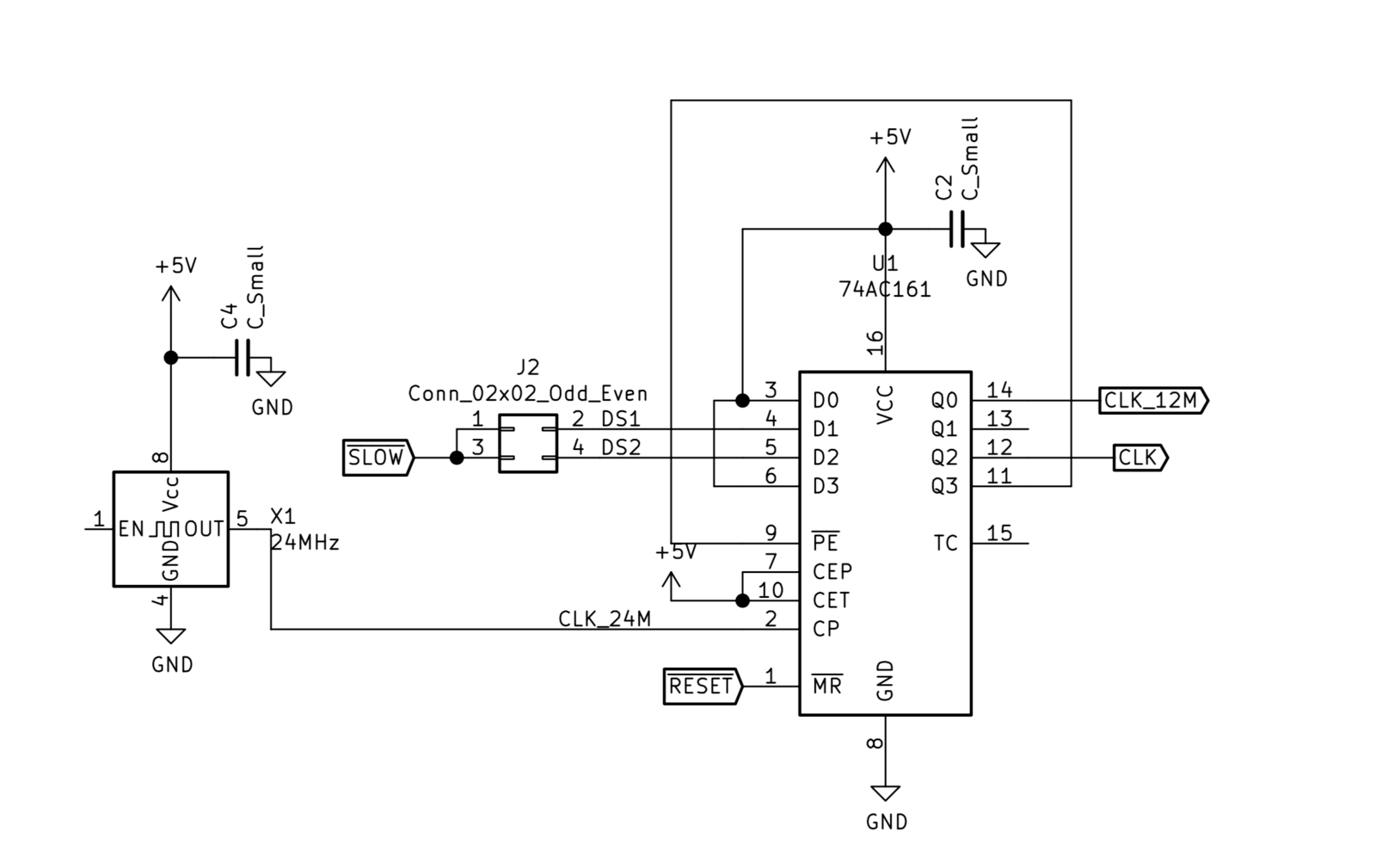
Let me explain this schematic: The 24Mhz output from the oscillator goes to the clock input of the binary counter. The Q0 output of the counter changes at every positive clock edge, so it is a square wave of half the frequency of the oscillator clock. This signal is fed to the expansion bus under the name CLK_12M. It is thus a non stretched clock that is used for things that require precises and consistent timings, such as VIA timers for example. Q3 is low when the counter is less than 8 and causes the counter to load its current count from the input. By default if the SLOW signal is high, then the counter will immediately load 15 and resume counting, which will take it back to zero, which will trigger the load again.
It that case the counter oscillates between 15 (all output high) and 0 (all outputs low) which causes CLK and CLK_12M to oscillate at the same frequency.
However, if the SLOW signal is asserted (low) than a number less than 15 will be loaded in the counter, which mean the Q2 (CLK signal) will toggle at a reduced frequency.
So this simple circuit generates two clock signal : one that is slow enough for the currently addressed peripheral, and one that is stable for timing sensitive peripherals. This also means that any timing sensitive peripherals MUST be able to run at the main (CLK) frequency.
Board connection
The Planck coomputer can be easily extended. It does this by means of an extension bus connector based on a 2.54mm 2x25 pins socket. These connectors are cheap, reliable and easy to obtain. The female connector is placed on the main board and a right angle male connector on each expansion board.
Most pins on this extension consist of the 65C02 signals, such as 16 address lines, 8 data lines, and a smattering of control lines. The complete bus pinout is detailed below:
| Pin number | Pin name | Description |
|---|---|---|
| 1 | A0 | Processor address bus pin 0 |
| 2 | D0 | Processor data bus pin 0 |
| 3 | A1 | Processor address bus pin 1 |
| 4 | D1 | Processor data bus pin 1 |
| 5 | A2 | Processor address bus pin 2 |
| 6 | D2 | Processor data bus pin 2 |
| 7 | A3 | Processor address bus pin 3 |
| 8 | D3 | Processor data bus pin 3 |
| 9 | A4 | Processor address bus pin 4 |
| 10 | D4 | Processor data bus pin 4 |
| 11 | A5 | Processor address bus pin 5 |
| 12 | D5 | Processor data bus pin 5 |
| 13 | A6 | Processor address bus pin 6 |
| 14 | D6 | Processor data bus pin 6 |
| 15 | A7 | Processor address bus pin 7 |
| 16 | D7 | Processor data bus pin 7 |
| 17 | A8 | Processor address bus pin 8 |
| 18 | EX0 | Extra pin for future use or for communication between expansion cards |
| 19 | A9 | Processor address bus pin 9 |
| 20 | EX1 | Extra pin for future use or for communication between expansion cards |
| 21 | A10 | Processor address bus pin 10 |
| 22 | SLOW | Used by slow peripherals to request a slower clock speed, active low. |
| 23 | GND | Ground |
| 24 | +5V | Positive voltage |
| 25 | +5V | Positive voltage |
| 26 | GND | Ground |
| 27 | A11 | Processor address bus pin 11 |
| 28 | SSEL | An expansion card is selected. Used by the processor card to disable it’s built-in ram and ROM, active low |
| 29 | A12 | Processor address bus pin 12 |
| 30 | INH | When this is active (low), processor card RAM and ROM are disabled |
| 31 | A13 | Processor address bus pin 13 |
| 32 | SLOT_SEL | Used by the main board to signal to expansion cards when they should activate, active low |
| 33 | A14 | Processor address bus pin 14 |
| 34 | LED1 | Connected to one of the backplane LEDs |
| 35 | A15 | Processor address bus pin 15 |
| 36 | LED2 | Connected to one of the backplane LEDs |
| 37 | RDY | Processor I/O pin. When low, the processor waits in its curent state |
| 38 | LED3 | Connected to one of the backplane LEDs |
| 39 | BE | Processor input pin. when low the processor releases the bus |
| 40 | LED4 | Connected to one of the backplane LEDs |
| 41 | CLK | Main computer clock. Can be stretched or not depending on the state of the SLOW signal. |
| 42 | CLK_12M | Stable clock for e.g. VIA timers. Not connected to slot 0 |
| 43 | RW | CPU read / write pin |
| 44 | EX2 | Extra signal 2. Not connected to slot 0 |
| 45 | IRQ | This goes low when an interrupt request has occured, active low |
| 46 | EX3 | Extra signal 3. Not connected to slot 0 |
| 47 | SYNC | CPU output. Indicates when the CPU is fetching an opcode |
| 48 | SLOT_IRQ | Used by expansion cards to signal an interrupt request to the processor board, active low |
| 49 | RESET | Reset signal trigered by the button on the backplane, active low |
| 50 | NMI | non maskable interrupt signal trigered by the button on the backplane, active low |
Expansion slot activation
The 65C02 works with memory mapped input/output. This means that the CPU does not care what device is responding to what address range. To it, when it asks for data from a certain address, it’s all the same whether that data comes from RAM, ROM, a temperature sensor or whetever else. This means that we need some external logic to activate certain devices when the CPU requests data from an address where we want that device to take control.
In our case, the backplane has some logic that tells one of the expansion slots to activate when a certain address range is requested by the CPU. This address decoding, as it is called is taken care of by an ATF22V10, a programmable logic chip that can be thought of as an ancestor to FPGAs.
This functionality could also be built from discrete logic chips, but using a PLD chip does three things for us:
- First it saves board space. The functionality this single chip provides would need at least two or three to replicate with discrete logic
- Secondly, it speeds up the response time. Each time a signal passes through a chip, it incurs a slight delay. So the fewer chips are on the path, the faster our computer can run.
- Finally, it allows us to reprogram it to easily change the memory map of the system.
In the default case, slot 1 responds in the address range $FF80 to $FF8F, slot 2 to $FF90 to $FF9F, etc until slot 5 at $FFC0 to $FFCF. This address decoding can be reconfigured by simply reprogramming the PLD, giving quite a lot of flexibility to the system.
Here is the default expansion memory map in table form
| START ADDRESS | END ADDRESS | DESCRIPTION |
|---|---|---|
| 0xFF80 | 0xFF8F | SLOT1 Selected |
| 0xFF90 | 0xFF9F | SLOT2 Selected |
| 0xFFA0 | 0xFFAF | SLOT3 Selected |
| 0xFFB0 | 0xFFBF | SLOT4 Selected |
| 0xFFC0 | 0xFFCF | SLOT5 Selected |
Basic user IO
The mainboard provides some basic user input and output in the form of two buttons and 4 leds.
The two buttons are a reset button and an NMI (non maskable interrupt) buttons. The reset button triggers a hard reset of the processor, whereas the NMI button provides a non maskable interrupt to the code that can be handled as a soft reset by the code.
The 4 LEDs are connected to pins on the expansion bus, and can thus be driven by any card that wants to signal something to the user. You have to be midful in your code not to drive a led low while another card is trying to drive it high, as that would cause very high current to flow into / from your peripherals.
Finally, there is a power plug (Barrel jack), a power switch and a power LED.
If you want to build this computer, please see the building the computer page to get more details about what to expect.
Serial IO
Included on the main board is a WDC 6552 serial interface. Its signals are brought out to a pin header into which a USB to serial adapter can be pluged.
RAM and ROM
32K of RAM and ROM are provided. The RAM socket allows for narrow or wide ram to be used.