CPU board
The CPU board contains the 65C02 cpu itself, but also 32K of ROM and 32K of RAM as well as the address decoding to handle these.
The address decoding is provided by a PLD, more specifically an ATF16V8. This chip also handles the incoming interrupt requests from the expansion card before passing them on to the CPU such that each extension card can send it’s own IRQ signal without risking contention with other cards.
The RAM can be either a wide or a narrow DIP chip, like the narrow IDT71256 or a more “classic” wide 62256 chip. The ROM placement on the board can accomodate a ZIF socket to allow the user to more easily update the software on the chip.
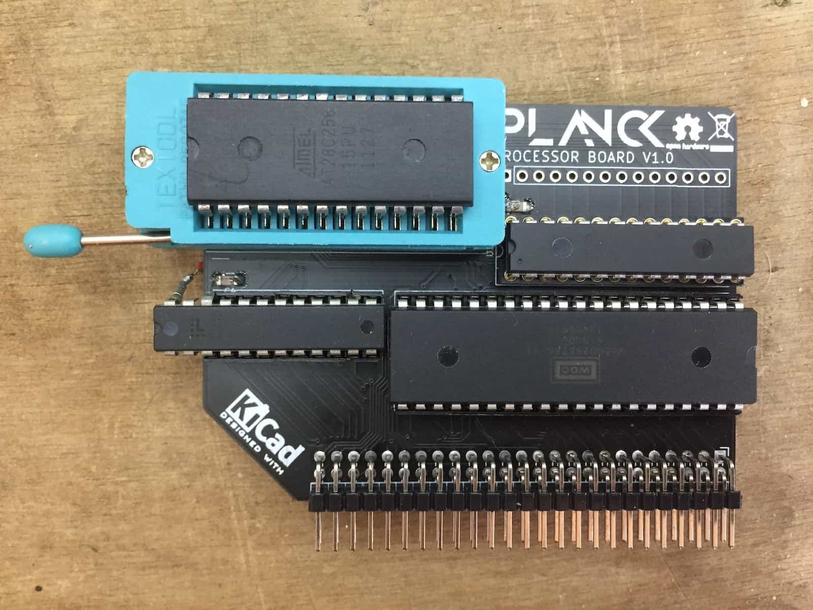
In this picture, you can see the 32k ROM chip in its ZIF socket at the top left.
At the top right is the RAM. As you can see, an additional row of holes are provided to accomodate a wide socket in case that is the RAM you have.
Bottom row at the left, you can see the address deconding for the onboard RAM and ROM. It is supposed to be an ATF16V8, but I only had 22V10s on hand, so some pins stick out the board, and had to be conected via soldered wires.
Finally at the bottom left in the 65C02 CPU.
Slot placement
The CPU board MUST be inserted in SLOT 0, marked CPU BOARD on the backplane.