CompactFlash card on the 65C02 CPU
After struggling for a long time with my prototype CompactFlash board, it turns out that once the design was put onto a PCB (and a few corrections made), everything worked flawlessly.
Hardware
You can get the full schematic for the CompactFlash board, but here is the gist of it:
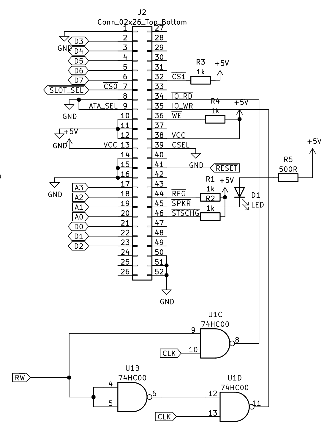
Basically, we connect all 8 data pins to the lower byte data pins on the CF card (CompactFlash works in 16 bit mode natively), and A0 to A3 to the lower four address lines of the CF card. Conveniently, the CompactFlash card in 8 bit mode requires only four address lines, which is exactly the address space that each expansion slots has available to it (16 bytes).
Then, we need to add some external ciruitry to convert the R/W signal and clock to the /IO_RD and /IO_WR signals that the CompactFlash card requires. This is just one NAND chip that set /IO_RD low when the R/W signal is high and the clock goes low, and set /IO_WR low when the R/W signal is low and the clock goes low.
The /CS0 signal is simply wired to the /SLOT_SEL signal from the bus, so that the CF card is selected whenever it’s slot is selected.
/CS1 is hard wired to a high signal, because it is only used in 16 bit mode (as far as I could make out).
Here is the first version that worked properly:
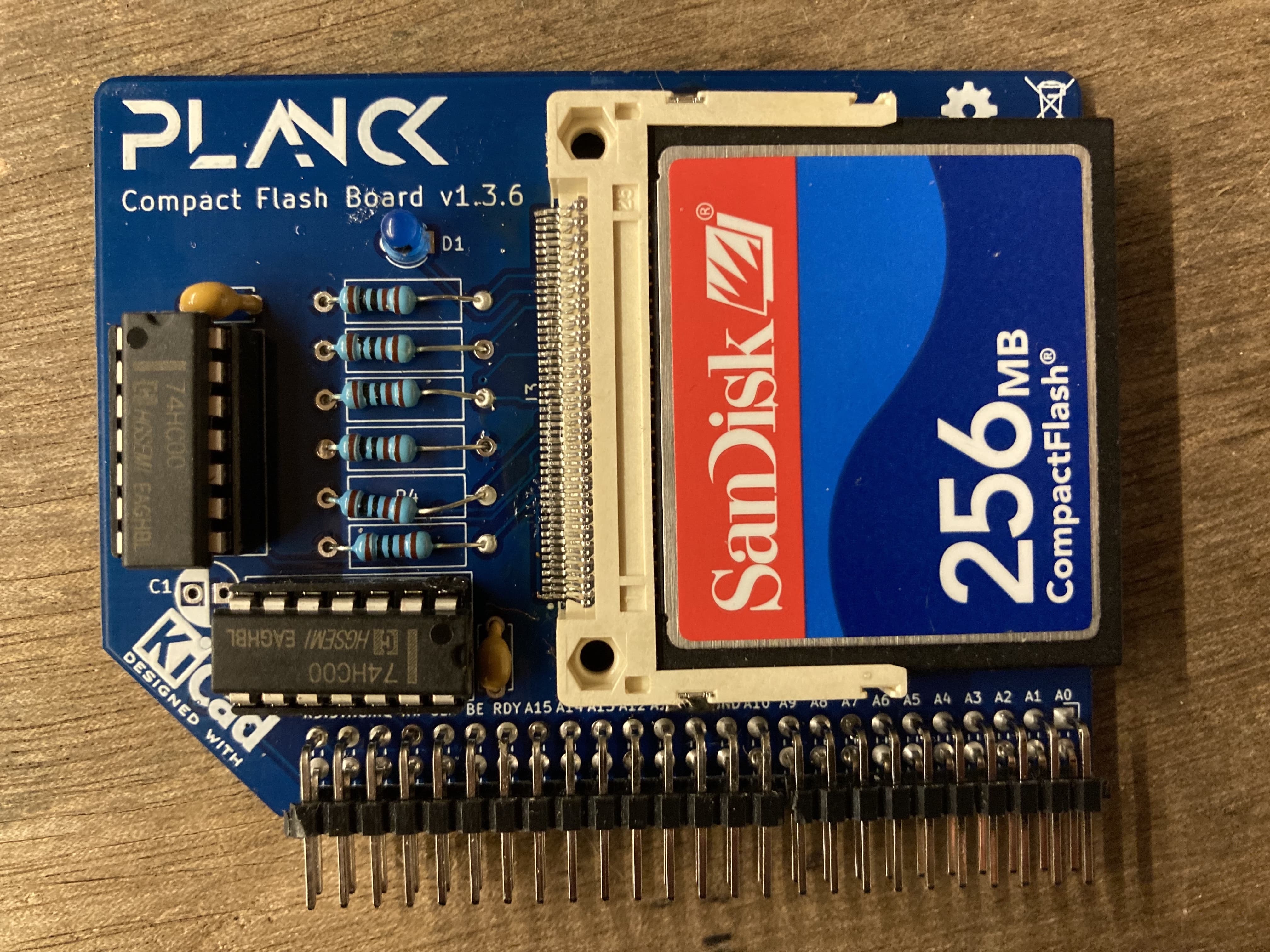
This is it for the hardware.
Software
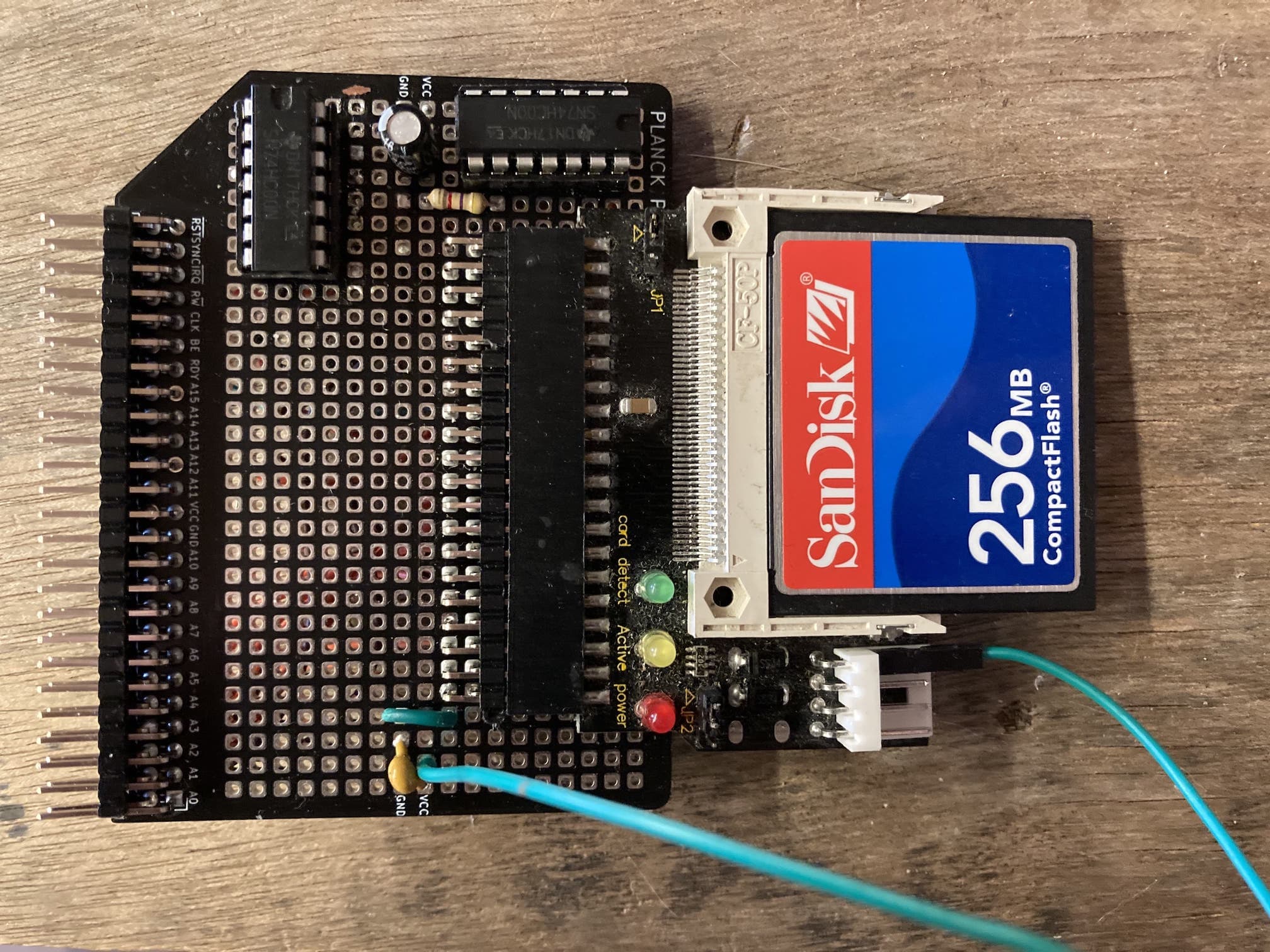
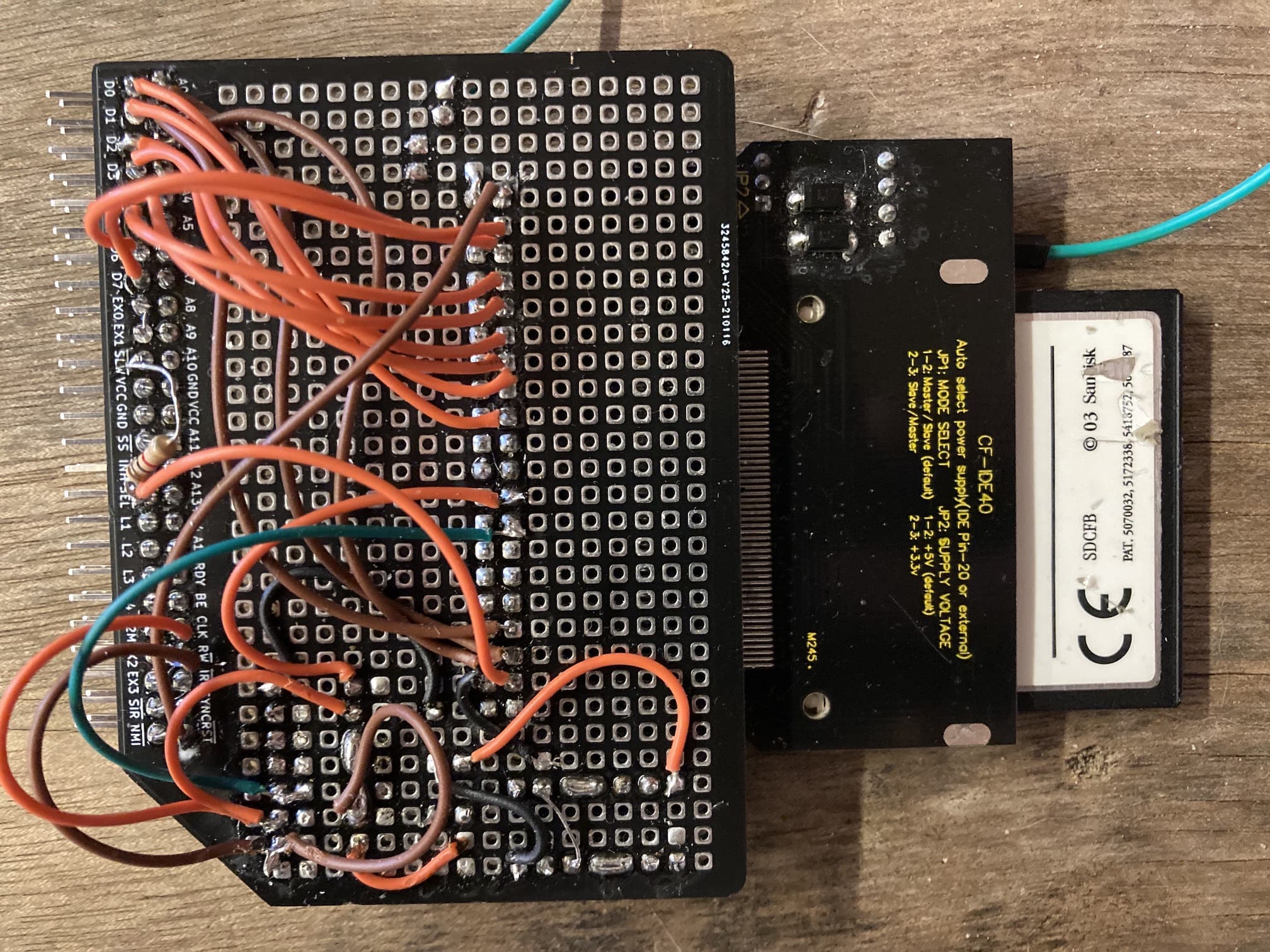
This is where I strugled pointelessly for a few weeks. With my prototype board (this one with a CF to IDA adapter and a mess of wires), I was getting spurious reads, some bytes would repeat, or not appear at all, and minute changes to the code would produce completely unexpected results… But as it turned out, it was just due to signal integrity issues. Here is the front and back of the prototype board:
Thankfully, the final CompactFlash board works perfectly.
So anyway, the code to read data from the CF card is pretty simple:
cf_read_sector:
    jsr cf_set_lba
    lda #1
    sta CF_ADDRESS + 2
    jsr cf_wait
    lda #CF_READ_SECTOR_COMMAND
    sta CF_ADDRESS + 7
    jsr cf_wait
    jsr cf_read
    jsr cf_err
    rts
This is the basic routine to trigger a sector read. It first calls the cf_set_lba routine which is as follows:
cf_set_lba:
    lda IO_SECTOR
    sta CF_ADDRESS + 3
    jsr cf_wait
    lda IO_SECTOR + 1
    sta CF_ADDRESS + 4
    jsr cf_wait
    lda IO_SECTOR + 2
    sta CF_ADDRESS + 5
    jsr cf_wait
    lda IO_SECTOR + 3
    and #$0F
    ora #$E0
    sta CF_ADDRESS + 6
    jsr cf_wait
    rts
Basically, it takes a 32 bit sector number from IO_SECTOR ans stores it into registers 3, 4, 5 and 6 of the CF card. The store in register 6 keeps only the lower 4 bits (a sector address is 28 bits) and set the high nybble to $E. I do not remeber exactly what that does, but the CompactFlash documentation I found explains it.
Then the cf_read_sector stores the number of sectors to read into the CF card register 2 (in our case a 1 as we wish to read a single sector). Then it waits until the card is ready (cf_wait is described below), and then sets the command (read sector, $20) into register 7. We then wait again until the card is ready, and then trigger the read proper. This is done by the following routine:
cf_read:
    phy
    ldy #0
@loop:
    jsr cf_wait
    lda CF_ADDRESS
    sta (io_buffer_ptr), y
    iny
    bne @loop
    inc io_buffer_ptr + 1
@loop2:
    jsr cf_wait
    lda CF_ADDRESS
    sta (io_buffer_ptr), y
    iny
    bne @loop2
    dec io_buffer_ptr + 1
@loop3:
    jsr cf_wait
    lda CF_ADDRESS + 7
    and #$08
    beq @exit
    lda CF_ADDRESS
    iny
    bne @loop3
@exit:
    ply
    rts
In this routine, we read the data register from the CF card repeatedly, until one page is complete (waiting for the card to be ready between each byte), and then we read the next page is the same way. Finally we read some more data until the card signals the end of the sector by setting bit 3 of the command register. The 512 byte buffer pointed to by io_buffer_ptr now contains one sector of data from the CompactFlash card!
Here is the cf_wait routine:
cf_wait:
    lda CF_ADDRESS + 7
    bmi cf_wait
    rts
Basically, we wait until bit 7 of the command register is unset to proceed.
And finally the cf_err routine, which is called at the end of the cf_read_sector routine
cf_err:
    jsr cf_wait
    lda CF_ADDRESS + 7
    and #$01
    beq @exit
@exit_fail:
    lda #'!'
    jsr kernel_putc
@exit:
    rts
This routine waits for the card to be ready, then check if bit 0 of the command register is set and if so prints one ! to indicate that an error has occurred, and otherwise does nothing.
And with that, we can now read data from a CompactFlash card with our humble 6502 processor (or in our case a 65C02).
Hopefully, this will give you some ideas for your own computer. You can also check the finalised CompactFlash board. And a big thank you to everyone on the 6502.org forum that gave tips and invaluable help.