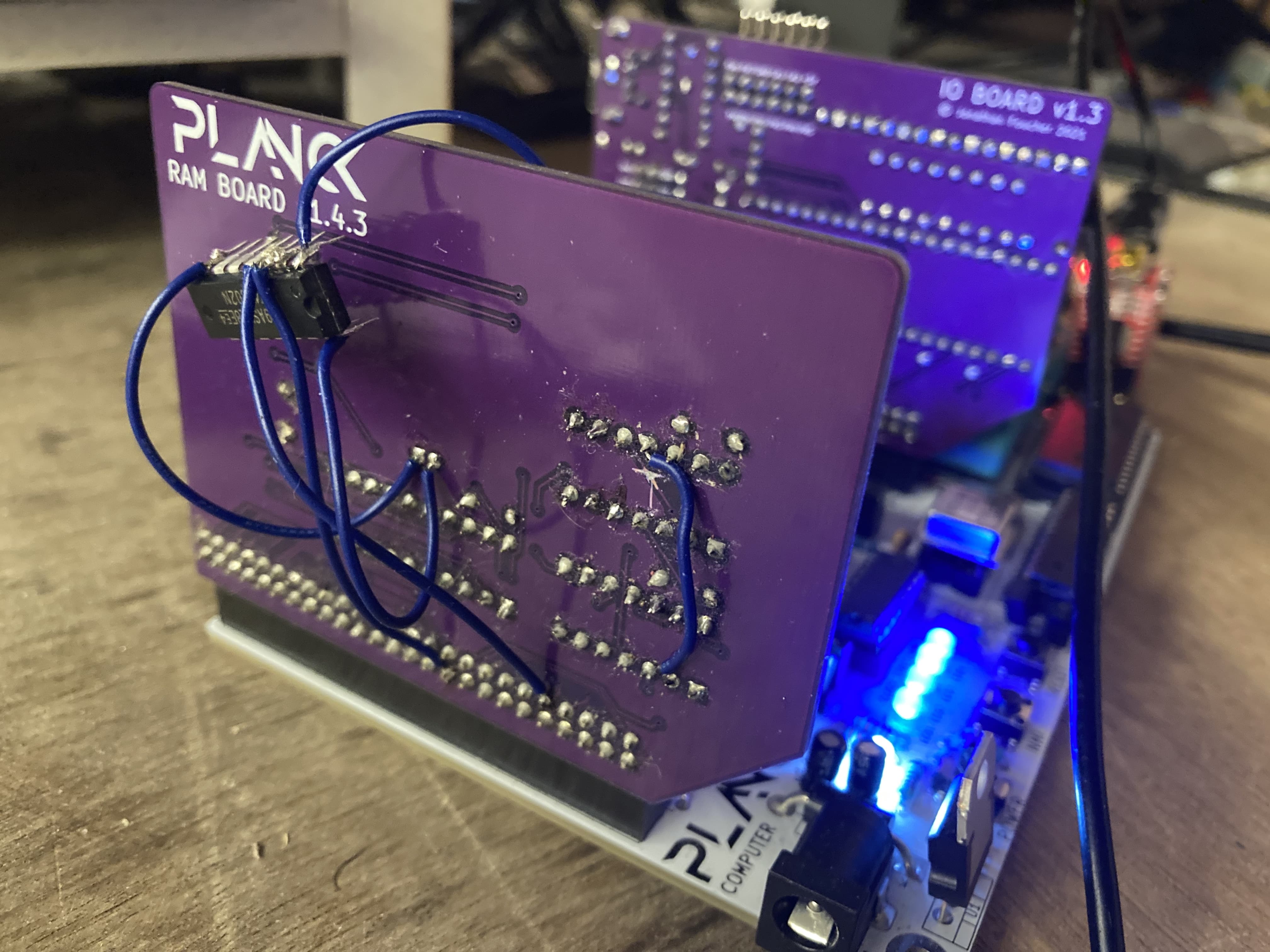
Good progress on the RAM board
The boards I had made for the RAM expansion board prototype were not working properly. It’s been a few months already, but I have not gone around to trying to fix it until now.
It turns out the logic to latch the bank register was wrong. I was NANDing the SLOT_SEL and clock signals together, which of course gave a square wave at the frequency of the clock itself. I should have spotted that to have a high signal when both the clock and SLOT_SEL signals go down, an NOR gate is sufficient.
So I scraped a few traces off, added a 74HC02 hanging in mid-air, and everything works perfectly now !!

The board Kicad files and gerbers will be updated soon.
I have also added a few words to the Forth firmware, namely expad which allows to set the slot where the ram board is located (run hex ffd0 expad if the board is in Slot 5 for example) and bank to activate / deactivate and set set the current bank.
0 bank will deactivate the expansion RAM and reactivate the ROM. hex 80 bank will deactivate the ROM between $8000 and $BFFF and place bank 0 of the RAM there.
The high bit of the value determines if the RAM is active or not (top bit set : RAM active, ROM deactivated, top bit unset : RAM deactivated, ROM active)
It is not possible to read the RAM expansion card register to check which bank is active, so your code should remember this information
